Researchers develop scalable approach to integrate ultrafast 2D flash memories
The widespread use of artificial intelligence (AI) tools designed to process large amounts of data has increased the need for better performing memory devices. The data storage solutions that could help to meet the computational demands of AI include so-called high-bandwidth memories, technologies that can increase the memory bandwidth of computer processors, speeding up the transfer of data and reducing power consumption.
Currently, flash memories are the most prominent memory solutions capable of storing information when a device is turned off (i.e., non-volatile memories). Despite their widespread use, the speed of most existing flash memories is limited and does not best support the operation of AI.
In recent years, some engineers have thus been trying to develop ultrafast flash memories that could transfer data faster and more efficiently. Two-dimensional (2D) materials have shown promise for fabricating these better performing memory devices.
While some long-channel flash-memory devices assembled from exfoliated 2D materials have been found to exhibit ultrafast processing speeds, the scalable integration of these devices has so far proven challenging. This has so far limited their large-scale commercialization and deployment.
Researchers at Fudan University recently devised a new approach for the scalable integration of ultrafast 2D flash memory devices. This approach, outlined in a paper in Nature Electronics, was effectively used to integrate 1,024 flash-memory devices with a yield of over 98%.
“Two-dimensional (2D) materials could potentially be used to create ultrafast flash memory,” wrote Yongbo Jiang, Chunsen Liu, and their colleagues in their paper. “However, due to interface engineering problems, ultrafast non-volatile performance is presently restricted to exfoliated 2D materials, and there is a lack of performance demonstrations with short-channel devices. We report a scalable integration process for ultrafast 2D flash memory that can be used to integrate 1,024 flash-memory devices with a yield of over 98%.”
To fabricate their ultrafast flash-memory array, the researchers used a combination of processing techniques, including lithography, e-beam evaporation, thermal atomic layer deposition, a polystyrene-assisted transfer technique and an annealing process. As part of their recent study, they applied their proposed approach to the fabrication of memories with two distinct memory stack configurations, both of which attained high yields.
“We illustrate the approach with two different tunneling barrier configurations of the memory stack (HfO2/Pt/HfO2 and Al2O3/Pt/Al2O3) and using transferred chemical vapor deposition-grown monolayer molybdenum disulfide,” wrote the researchers.
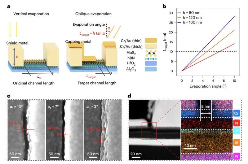
“We also show that the channel length of the ultrafast flash memory can be scaled down to sub-10 nm, which is below the physical limit of silicon flash memory. Our sub-10 nm devices offer non-volatile information storage (up to 4 bits) and robust endurance (over 105).”
Initial tests run by Jiang, Liu and their colleagues demonstrated the promise of their approach for the scalable integration of ultrafast flash memories attaining high yields. The researchers successfully scaled the channel length of their flash memories down to sub-10 nm and found that these sub-10 nm devices still exhibited ultrafast speeds, storing up to 4 bits and maintaining their non-volatility.
Further studies could use the team’s proposed integration process to fabricate flash memory arrays based on other 2D materials and with varying memory stack configurations. These efforts could further contribute to the future large-scale deployment of ultrafast flash memory devices.
More information:
Yongbo Jiang et al, A scalable integration process for ultrafast two-dimensional flash memory, Nature Electronics (2024). DOI: 10.1038/s41928-024-01229-6
© 2024 Science X Network
Citation:
Researchers develop scalable approach to integrate ultrafast 2D flash memories (2024, September 14)
retrieved 15 September 2024
from https://techxplore.com/news/2024-09-scalable-approach-ultrafast-2d-memories.html
This document is subject to copyright. Apart from any fair dealing for the purpose of private study or research, no
part may be reproduced without the written permission. The content is provided for information purposes only.

Comments are closed