New material design for transistors could downsize next-gen tech
By better taming the Jekyll-and-Hyde nature of an alternative to the semiconductor—one that transitions from electricity-resisting insulator to current-conducting metal—Nebraska’s Xia Hong and colleagues may have unlocked a new path to smaller, more efficient digital devices. The team reports its findings in the journal Nature Communications.
The semiconductor’s ability to conduct electricity in the Goldilocks zone—poorer than a metal, better than an insulator—positioned it as the just-right choice for engineers looking to build transistors, the tiny on-off switches that encode the 1s and 0s of binary. Apply some voltage to the control knob known as a gate insulator, and the semiconductor channel allows electric current to flow (1); remove it, and that flow ceases (0).
Millions of those nanoscopic, semiconductor-based transistors now coat modern microchips, switching on and off to collectively process or store data. But as minuscule as the transistors already are, the demands of consumers and competition continue pushing electrical engineers to shrink them even further, either for the sake of squeezing in more functionality or downsizing the devices that house them.
Unfortunately, those engineers are now bumping up against the practical and even fundamental limits of just how small semiconductors can get.
Researchers, in turn, have begun looking beyond not just industry favorite silicon but semiconductors as a whole. More than two decades ago, some began tooling around with a class of materials called Mott insulators. If the semiconductor is the happy medium that has driven decades of clockwork-constant progress, the Mott insulator is more akin to a two-faced wild card whose ambivalence rates as both the source of its appeal and of frustration.
A longstanding theory of conductivity says that a material with the electronic characteristics of a Mott insulator should generally be classified as a metal. Unlike the electrons in a metal or semiconductor, though, those in a Mott insulator don’t behave like independent particles.
Instead, they interact in ways that confine them to localized sites and keep them from moving freely through a material. Still, certain conditions—higher temperatures, the introduction of more electrons—can overwhelm those forces, ultimately freeing the electrons and essentially transforming the Mott insulator into a conductive metal.
“So you (traditionally) have either itinerant electrons or localized electrons,” said Hong, professor of physics at the University of Nebraska–Lincoln. “It’s very clearly defined.”
“But in the case of a Mott insulator, electron interactions cannot be ignored. Because of that correlation, it’s hard to define it as simply a metal or insulator. If you can tune the strength of the interaction, it can be a metal, or it can be an insulator.”
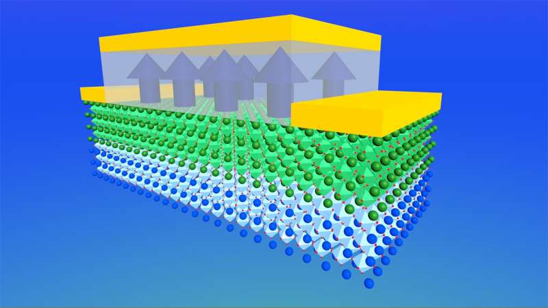
By topping a Mott insulator with a gate insulator made of so-called ferroelectric material—then using voltage to flip the latter’s polarization, or alignment of positive and negative charges—researchers realized they could direct the Mott transition from insulator to metal and back again. In that way, the pairing’s behavior, and most promising function, took after that of the semiconductor.
More information:
Yifei Hao et al, Record high room temperature resistance switching in ferroelectric-gated Mott transistors unlocked by interfacial charge engineering, Nature Communications (2023). DOI: 10.1038/s41467-023-44036-x
University of Nebraska-Lincoln
Citation:
New material design for transistors could downsize next-gen tech (2024, February 2)
retrieved 2 February 2024
from https://techxplore.com/news/2024-02-material-transistors-downsize-gen-tech.html
This document is subject to copyright. Apart from any fair dealing for the purpose of private study or research, no
part may be reproduced without the written permission. The content is provided for information purposes only.

Comments are closed