Engineers develop new two-dimensional, low-power-consumption field-effect transistor
A team of electrical and computer engineers at Shanghai Institute of Microsystem and Information Technology, Chinese Academy of Sciences, working with one colleague from City University of Hong Kong and another with Fudan University, has developed a new two-dimensional, low-power-consumption field-effect transistor (FET) that could allow smartphones to need recharging less often.
In their paper published in the journal Nature, the group describes how they overcame problems with high gate leakage and low dielectric strength that have stymied other researchers looking to create smaller and thinner computer chips. Two of the team members (Ziao Tian and Zengfeng Di) have published a Research Briefing, summarizing their work in the same journal issue.
Over the past several years, computer engineers have been searching for new materials that will allow further miniaturization of silicon field-effect transistors. This will enable the addition of more features in phones and other devices without making them bigger. It is also a necessity for the development of 5G devices that will come with AI applications that are still in development.
There is also expected to be a need to reduce the size of devices used in IoT applications. Notably, current materials have already begun to suffer from short-channel effects. Many in the field have seen 2D materials as the future for such devices because they would allow for reducing thickness to just a few atoms.
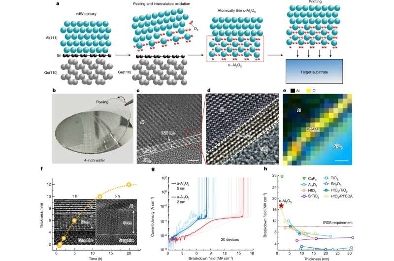
Unfortunately, most such efforts have had issues with smooth interactions between the 2D materials and other parts that must connect to them. More recently, some researchers have begun to look at thin metal oxides as a possible solution. In this new effort, the research team has used single-crystalline aluminum oxide just 1.25 nm thick.
The researchers note that each of the FETs they created had an aluminum gate just 100 µm wide and 250 nm long. To ensure complete insulation, they left a gap between the gates. To create their FETs, they used standard van der Waals transfer methods to properly align the materials on the underlying wafer before moving the stack over as a single step. The team describes the resulting product as a 2D FET with high-quality dielectric interfaces.
More information:
Daobing Zeng et al, Single-crystalline metal-oxide dielectrics for top-gate 2D transistors, Nature (2024). DOI: 10.1038/s41586-024-07786-2
Ultrathin sapphire synthesized for advanced 2D electronics, Nature (2024). DOI: 10.1038/d41586-024-02634-9
© 2024 Science X Network
Citation:
Engineers develop new two-dimensional, low-power-consumption field-effect transistor (2024, August 26)
retrieved 27 August 2024
from https://techxplore.com/news/2024-08-dimensional-power-consumption-field-effect.html
This document is subject to copyright. Apart from any fair dealing for the purpose of private study or research, no
part may be reproduced without the written permission. The content is provided for information purposes only.

Comments are closed