Electronics engineers successfully integrate MoS₂ transistors on a 200 mm wafer
In recent years, electronics engineers have been trying to design increasingly sophisticated transistors that can be scaled down to smaller sizes. Given the limitations of conventional silicon-based field effect transistors (FETs), some teams have been experimenting with alternative designs based on materials with higher electron mobility.
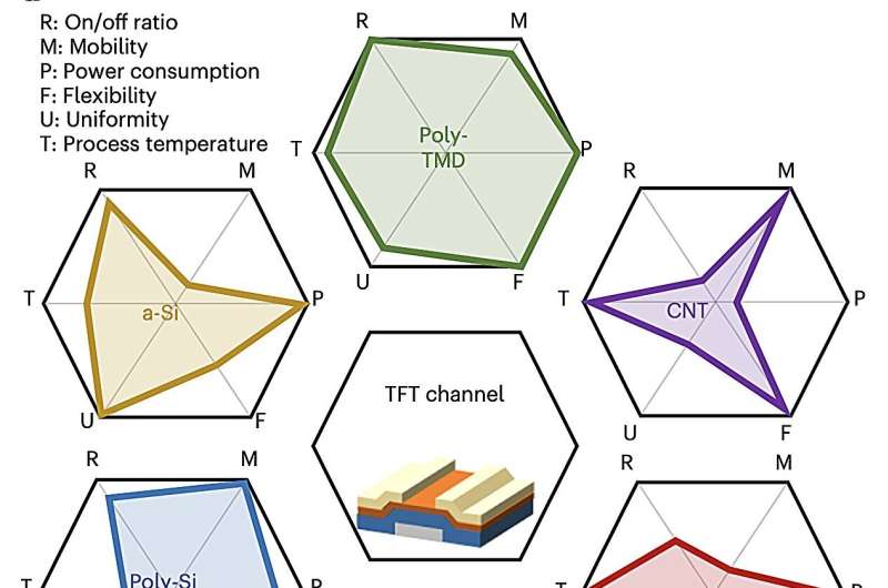
Transition metal dichalcogenides (TMDs) are among the most promising materials for the development of scalable FETs, due to their small length and good carrier mobility. One of these materials is molybdenum disulfide (MoS2), a compound consisting of molybdenum and sulfide atoms in a 1:2 ratio.
Researchers at Samsung Advanced Institute of Technology (SAIT) and Seoul National University recently demonstrated integration of MoS2 transistors on a 200 mm wafer. Their paper, published in Nature Electronics, demonstrates the scalability of transistors based on MoS2, highlighting their potential for the future development of smaller and flexible devices.
“Two-dimensional semiconductors are an attractive material for making thin-film transistors due to their scalability, transferability, atomic thickness and relatively high carrier mobility,” Junyoung Kwon, Minsu Seol, and their colleagues wrote.
“There is, however, a gap in performance between single-device demonstrations, which typically use single-crystalline two-dimensional films, and devices that can be integrated on a large scale using industrial methods. We report the 200-mm-wafer-scale integration of polycrystalline MoS2 field-effect transistors.”
The team first fabricated large-scale arrays of MoS2 FETs using a technique known as metal-organic chemical vapor deposition (MOCVD). The team was able to eliminate the so-called Schottky barrier at the interface between the MoS2 material and metal, which enhanced the FETs’ carrier mobility.
Notably, the fabrication strategy they employed is compatible with current processes used to manufacture electronics. In fact, the researchers processed their FETs at a commercial facility, achieving a yield of over 99.9%.
“We find that the metal–semiconductor junction in polycrystalline MoS2 is fundamentally different from its single-crystalline counterpart, and therefore, we redesign the process flow to nearly eliminate the Schottky barrier height at the metal–MoS2 contact,” the researchers wrote in their paper.
“The resulting MoS2 FETs exhibit mobilities of 21 cm2 V−1 s−1, contact resistances of 3.8 kΩ µm and on-current densities of 120 µA µm−1, which are similar to those achieved with single-crystalline fakes.”
In initial tests, the FETs designed and fabricated by this team of researchers achieved highly promising results, outperforming other previously introduced FETs based on MoS2 in terms of field-effect mobility, contact resistance, and on-current densities. The team attributed the FETs remarkable performance to the new fabrication steps they introduced, which eliminated the Schottky barrier at the MoS2/metal interface and reduced contact resistance.
In addition, the team identified various factors that could contribute to reported differences between their devices’ performance and yield compared to those of previously developed MoS2-FETs. These include a lack of impurities on the contact and the prevention of MoS2 materials peeling off.
When they integrated their FETs on a 200 mm wafer, the researchers found that they were uniform, only exhibiting slight die-to-die variations. Moreover, they demonstrated the feasibility of reliably fabricating their FETs at existing industrial facilities.
In the future, their study could inspire other teams to experiment with similar FET designs and fabrication processes. Ultimately, this could facilitate the development and large-scale commercialization of highly performing transistors based on MoS2.
More information:
Junyoung Kwon et al, 200-mm-wafer-scale integration of polycrystalline molybdenum disulfide transistors, Nature Electronics (2024). DOI: 10.1038/s41928-024-01158-4.
© 2024 Science X Network
Citation:
Electronics engineers successfully integrate MoS₂ transistors on a 200 mm wafer (2024, May 20)
retrieved 21 May 2024
from https://techxplore.com/news/2024-05-electronics-successfully-mos-transistors-mm.html
This document is subject to copyright. Apart from any fair dealing for the purpose of private study or research, no
part may be reproduced without the written permission. The content is provided for information purposes only.

Comments are closed