Cost effective method developed for co-packaging photonic and electronic chips
The future of digital computing and communications will involve both electronics—manipulating data with electricity—and photonics, or doing the same with light. Together the two could allow exponentially more data traffic across the globe in a process that is also more energy efficient.
“The bottom line is that integrating photonics with electronics in the same package is the transistor for the 21st century. If we can’t figure out how to do that, then we’re not going to be able to scale forward,” says Lionel Kimerling, the Thomas Lord Professor of Materials Science and Engineering at MIT and director of the MIT Microphotonics Center.
Enter FUTUR-IC, a new research team based at MIT. “Our goal is to build a microchip industry value chain that is resource-efficient,” says Anu Agarwal, head of FUTUR-IC and a principal research scientist at the Materials Research Laboratory (MRL).
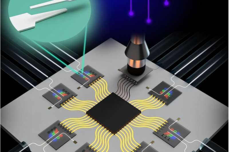
Now, FUTUR-IC researchers including Agarwal and Kimerling have developed a new way to co-package photonic chips with their electronic counterparts that solves several problems associated with the current co-packaging process. One advantage is that the newly developed co-packaged device can be manufactured using existing equipment in traditional electronics foundries with a less-expensive passive alignment process. As a result, the MIT solution promises to be cost-effective.
A paper on the device, which is patented, was featured on the cover of Advanced Engineering Materials earlier this year. Last fall another paper on the work was presented by the lead author, Drew Weninger, at the 57th International Symposium on Microelectronics. Weninger, a graduate student in the Department of Materials Science and Engineering (DMSE), won the Best Student Paper Award at the event.
In addition to Weninger, Kimerling, and Agarwal, authors of the paper are Samuel Serna of Bridgewater State University and Luigi Ranno, a DMSE graduate student.
Toward a resource-efficient microchip industry
Consider the following: In 2020, the number of cell phones, GPS units, and other devices connected to the “cloud,” or large data centers, will exceed 50 billion, according to Kimerling. And data-center traffic, in turn, is scaling by 1,000 times every 10 years.
This communication consumes energy. And “all of it has to happen at a constant cost of energy, because the gross domestic product isn’t changing at that rate,” says Kimerling, who is also affiliated with the MRL. The solution is to either produce more energy or make information technology more energy efficient.
, the process flow used to fabricate and package the chip-to-chip coupling prototypes. In b), cross-sectional SEM images show the minimum and maximum feature sizes for the SOI and SiN 𝑥 . In c,d), the chip-to-chip prototype and separate glass chip on the testing stage. In e), a schematic of the testing setup. Credit: Advanced Engineering Materials (2024). DOI: 10.1002/adem.202402095")
Integrating photonics with the electronics that underpin today’s microchips could address the latter because the transmission, or communication, of data using light is much more energy efficient. “Our mantra is to use electronics for computation and photonics for communication to bring this energy crisis under control,” says Agarwal.
However, this solution comes with its own challenges.
For example, currently it is difficult and expensive to connect electronic chips with their photonic counterparts within a single package. That’s because the optical fiber, which has a core diameter of ten micrometers (ten millionths of a meter), and the photonic chip, which has cross-sectional dimensions of only two tenths by five tenths of a micrometer, must be aligned almost perfectly or the light will disperse. As a result, today each connection must be actively tested with a laser to ensure that the light will come through.
“And the number of fibers that we will need for greater data communication is increasing exponentially, so this active alignment process won’t cut it for scaling forward,” Weninger said.
More wiggle room
The new device, called an evanescent coupler, gives much more wiggle room for connecting the fibers within the electronic-photonic package. “Conventional couplers have a single coupling point, making alignment tolerances very tight. But our new coupler has a much larger interaction length increasing the alignment tolerance,” says Agarwal. As a result, robots could passively assemble the resulting integrated circuits allowing more light to pass through without being lost (no active laser alignment is needed).
Another key innovation: the coupler “allows us to transmit light vertically” between the multiple layers of chips that comprise the whole, says Ranno. That in itself is an important feat because it is difficult to direct light out of a horizontal plane.
“In electronics it is very simple. Electrons can easily flow out of plane,” Weninger says. In contrast, “light never wants to take right angles.” The new coupler lets light make the jump between stacked chips.
Ranno concludes, “We’ve developed a packaging design [for integrating photonics with electronics] that is reliable, has a larger alignment tolerance, doesn’t lose much light, and doesn’t waste too much space. Basically, it has all the features you want for an efficient and functional interconnect.”
This work was carried out in part through the use of facilities at MIT.nano, and includes contributions from MIT’s Electronic-Photonic Packaging Consortium.
More information:
Drew Weninger et al, Low Loss Chip‐to‐Chip Couplers for High‐Density Co‐Packaged Optics, Advanced Engineering Materials (2024). DOI: 10.1002/adem.202402095
Materials Research Laboratory, Massachusetts Institute of Technology
This story is republished courtesy of MIT News (web.mit.edu/newsoffice/), a popular site that covers news about MIT research, innovation and teaching.
Citation:
Cost effective method developed for co-packaging photonic and electronic chips (2025, July 28)
retrieved 29 July 2025
from https://techxplore.com/news/2025-07-effective-method-photonic-electronic-chips.html
This document is subject to copyright. Apart from any fair dealing for the purpose of private study or research, no
part may be reproduced without the written permission. The content is provided for information purposes only.
Comments are closed