A new strategy for fabricating high-density vertical organic electrochemical transistor arrays
Organic electrochemical transistors (OECTs) are an emerging class of transistors based on organic superconducting materials known for their ability to modulate electrical current in response to small changes in the voltage applied to their gate electrode. Like other electronics based on organic semiconductors, these transistors could be promising for the development of various brain-inspired and wearable technologies.
OECTs have various notable advantages, including promising amplification and sensing capabilities. low driving voltages, and a versatile structure. Despite these advantages, most conventional OECTs developed so far have been found to exhibit various limitations, including limited stability and slow redox processes, which can significantly impair their performance.
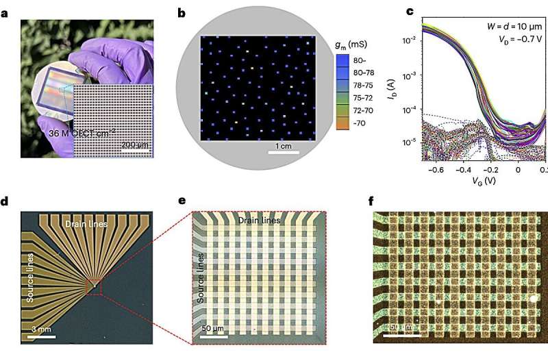
Researchers at Northwestern University recently outlined a new strategy to fabricate high-density and mechanically flexible OECTs. Their proposed approach, outlined in a paper in Nature Electronics, was used to create various electronic components based on OECT arrays and circuits.
“Organic electrochemical transistors (OECTs) can be used to create biosensors, wearable devices, and neuromorphic systems,” Jaehyun Kim, Robert M. Pankow, and their colleagues wrote in their paper.
“However, restrictions in the micro- and nanopatterning of organic semiconductors, as well as topological irregularities, often limit their use in monolithically integrated circuits. We show that the micropatterning of organic semiconductors by electron-beam exposure can be used to create high-density (up to around 7.2 million OECTs per cm2) and mechanically flexible vertical OECT arrays and circuits.”
To fabricate their OECT arrays, Kim, Pankow, and their colleagues first exposed both p- and n-channel organic semiconductor films to a direct beam of electrons. This method, known as electron beam lithography (eBL), allowed them to produce a pattern on the semiconducting films without employing masks or chemical solvents that could damage the materials. This made the films electronically inactive (i.e., insulating) without affecting their ability to conduct ions.
The patterned films resulting from this process were ultra-small and high-density while also presenting well-defined, conducting channel regions. Moreover, the eBL strategy employed by the researchers enabled the effective multilayer integration of OECT structures into arrays and circuits.
“The energetic electrons convert the semiconductor exposed area to an electronic insulator while retaining ionic conductivity and topological continuity with the redox-active unexposed areas essential for monolithic integration,” Kim, Pankow, and their colleagues wrote in their paper. “The resulting p- and n-type vertical OECT active-matrix arrays exhibit transconductances of 0.08–1.7 S, transient times of less than 100 μs and stable switching properties of more than 100,000 cycles.”
To further demonstrate the potential of their fabrication strategy, the researchers successfully used it to create various vertically stacked logic circuits based on their OECTs, including NOT, NAND, and NOR gates. The circuits they created were found to perform remarkably well while also maintaining excellent operational stability.
In the future, this recent study could inform the development of similar approaches to boost the stability and performance of OECT circuits. Moreover, the new e-beam exposure strategy it introduced could facilitate the scalable fabrication of OECTs, contributing to their integration into electronic devices.
More information:
Jaehyun Kim et al, Monolithically integrated high-density vertical organic electrochemical transistor arrays and complementary circuits, Nature Electronics (2024). DOI: 10.1038/s41928-024-01127-x
© 2024 Science X Network
Citation:
A new strategy for fabricating high-density vertical organic electrochemical transistor arrays (2024, March 31)
retrieved 1 April 2024
from https://techxplore.com/news/2024-03-strategy-fabricating-high-density-vertical.html
This document is subject to copyright. Apart from any fair dealing for the purpose of private study or research, no
part may be reproduced without the written permission. The content is provided for information purposes only.

Comments are closed