A method to rapidly align micro-light-emitting diodes at a wafer-scale
February 22, 2023
feature
Micro-light-emitting diodes (μLEDs) could have many valuable technological applications. For instance, they can be used to create highly efficient displays for smart phones, tablets and virtual reality displays, enhancing their image quality and resolution.
Fabricating displays based on μLEDs, however, is far from an easy task, as it requires the effective alignment and integration of millions of tiny LED devices at a wafer-scale. As a result of these challenges, these displays are still at very early stages of development.
Researchers at the Samsung Advanced Institute of Technology(SAIT), Chungbuk National University and Soongsil University recently devised FAST, a strategy to align μLEDs on chips both reliably and rapidly. This strategy, outlined in a paper published in Nature Electronics, could potentially enable the large-scale fabrication of new μLED-based displays for electronic devices.
“We have been working on the development of μLED for high-resolution displays, which are emerging as next generation displays,” KyungWook Hwang, SAIT researcher and one of the corresponding authors of the study, told Tech Xplore. “There have been difficulties in developing and even for commercializing these displays, due to various technical problems, including the creation of a transfer technology that can convey μLED onto a display substrate.”
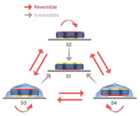
The key objective of the recent work by Hwang and his colleagues was to devise a mass transfer strategy that would allow them to move LEDs onto wafers more quickly and reliably than existing methods. The strategy they proposed relies on the control of the van der Waals force between chips and an interposer (i.e., intermediate electrical interface that routs between sockets or connections).
. Credit: Hwang et al")
“We had no prior knowledge of the transfer technology itself and no microLED chips to practice on, but I think that played a big part in finding differentiated new idea ‘FAST,'” Hwang said. “Our FAST technology is simple, thus is requires a shorter time for transfer, and it also can be used to make a large-area display as well, it is thought to be applicable to various applications. These features will also help speed up the wide adoption of technology.”
FAST, the strategy proposed by the researchers, entails the engineering of the upper and lower surfaces of μLED chips to attain different van der Waals forces. These forces allow the chips to selectively bond to substrates via fluidic and drying processes.
“I think the most remarkable achievement in our study is the unbiased acceptance of a new phenomenon in which electrodes were aligned in the upward direction of a substrate,” Hwang said. “Most of the groups that studied fluid alignment of microchips judged that it was right result for the electrodes of chip to be aligned in the bottom direction of substrate. But we have overcome prejudice against results of previous studies. If we had not challenged conventional wisdom, we would not have been able to come to a new conclusion.”
Using FAST, Hwang and his colleagues were able to irreversibly align 259,200 μLED chips with an accuracy of 100% and a transfer yield of 99.992% over 40 trials. In addition, they created a series of μLED-based passive and active-matrix displays, by bonding a μLED-loaded interposer to backplanes based on a low-temperature polysilicon thin-film transistor.
The strategy devised by this team of researchers is a significant step forward in the ongoing journey toward the large-scale fabrication and commercialization of high-performance displays based on μLEDs. In the future, it could be used to fabricate displays for different devices and might also inspire the development of other reliable μLED-integration methods.
“We now plan to create new opportunities for Si and more III-V devices through our ‘FAST’ method,” Hwang added. “Our approach could accelerate the development of next-generation μLEDs and can be used for the large-area transfer of all the devices, including III–V and 2D materials.”
More information:
Junsik Hwang et al, Wafer-scale alignment and integration of micro-light-emitting diodes using engineered van der Waals forces, Nature Electronics (2023). DOI: 10.1038/s41928-022-00912-w
© 2023 Science X Network
Citation:
A method to rapidly align micro-light-emitting diodes at a wafer-scale (2023, February 22)
retrieved 23 February 2023
from https://techxplore.com/news/2023-02-method-rapidly-align-micro-light-emitting-diodes.html
This document is subject to copyright. Apart from any fair dealing for the purpose of private study or research, no
part may be reproduced without the written permission. The content is provided for information purposes only.
Comments are closed