Fixing solar’s weak spot: Why a tiny defect could be a big problem for perovskite cells
A recent study provides evidence to help solve one of the key hurdles to large-scale manufacture of next-generation perovskite solar cells.
The work, a collaboration between a team led by RASEI Fellow Mike McGehee at the University of Colorado Boulder and scientists at the National Renewable Energy Laboratory (NREL), is published in the journal Joule.
Imagine you have a series of hoses connected end to end to water your garden. The water flows from the faucet, through each hose, and out the last nozzle. When every hose is getting enough water, the flow is strong and steady. This is like how a string of solar cells works on a solar panel; the sun’s energy makes electrons (the “water”) that flow through each cell, creating electricity.
But what happens if a single section of the hose gets kinked? The water can’t flow through it anymore, but there is still a lot of pressure coming from the faucet. The pressure will build up and eventually burst the weak spot in the kinked section. This is analogous to what happens when a section of the solar panel is shaded—the cell becomes kinked. When just one part of a panel is shaded, the unshaded cells still generate electricity and “force” current backward through the non-producing shaded cell. This is known as reverse bias, and it can cause the shaded cell to permanently degrade and fail.
For conventional silicon-based solar cells, reverse bias is a known problem and engineers have developed a solution: a bypass diode. You can think of this as a small side-channel that allows the water to flow around the kinked hose, keeping the rest of the system running smoothly without building up damaging pressure.
However, the bypass diode solution doesn’t work for perovskite-based solar cells, a leading candidate for the next generation of more efficient and more affordable solar cells, because they are often too “weak.” One of the key pieces in the puzzle to solving this reverse bias problem in perovskite solar cells is understanding how the cell degrades when under reverse bias, and that is the focus of this research collaboration.
The McGehee group has a long history of success in creating and optimizing perovskite solar cells. Beginning in 2018, their focus shifted to a critical challenge: what happens when these cells are in the shade? Many researchers had already observed that even a small amount of reverse bias caused the materials to heat up and “melt,” leading to rapid and permanent degradation of the perovskite.
While these observations were widely accepted, the exact reason for the degradation was a mystery and a subject of much debate.
“These are complex systems, and it can be very hard to untangle what is going on,” explained Ryan DeCrescent, one of the study’s lead researchers. This is where the McGehee group’s work came in—they set out to find the specific mechanism behind this destructive behavior.
The perovskite layer is formed through an approach called solution processing. Solution processing is kind of like making a pancake. You make your batter and when you pour it onto a hot griddle, several things happen: the water evaporates, the solids set, the thickness is determined by how much you add, and you often get gaps (holes) in your pancake.
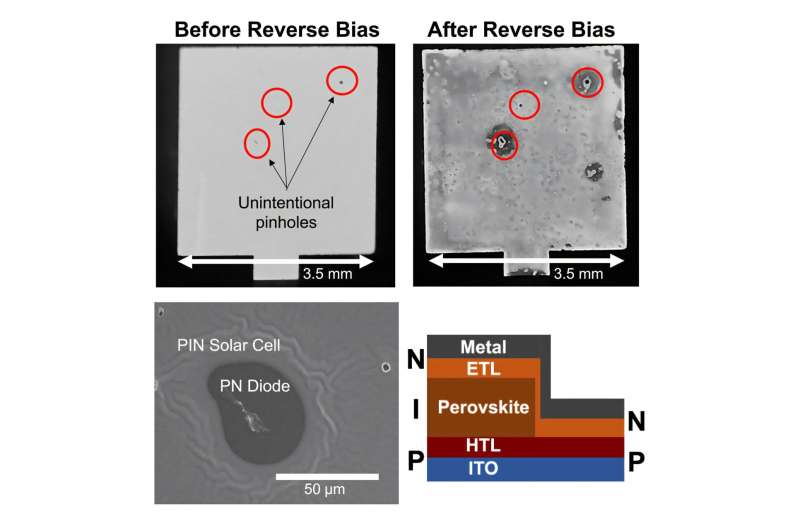
In these devices, the perovskite ingredients are put into a solvent. The solvent is then dropped onto the earlier layers of the device and warmed up, whereby the solvent evaporates and a film is formed, but often with defects, or gaps. Defects and pinholes are easily formed in such films. This is a particular issue for perovskites, since the precursor solution has low viscosity, and during the heating stage, defect formation is common.
To better understand the impact of these defects on the performance of the solar cells under reverse bias, you need to take a really good look at them. Central to this work is a suite of tools that enabled exceptional examination of the perovskite layer.
“A large part of this work was really setting ourselves up to look very carefully at these surfaces,” said DeCrescent.
Four main techniques were employed to better understand the defects: Electroluminescence (EL) imaging with a high-resolution camera, Scanning Electron Microscopy (SEM), Laser-Scanning Confocal Microscopy (LSCM) and Video Thermography. The strategy was to compare before-, during-, and after-pictures of devices that had been exposed to reverse bias. The high-resolution camera showed that weak spots in the device were the origin of degradation.
To better understand “perfect” device behavior and efficiently scan a large number of samples (~100), the team set up a large number of very small devices, creating thin films with an area of just 0.032 mm. To put that in perspective, each device was about the width of two human hairs. The small size of these devices meant that it was possible to create devices that were defect-free, since it is hard to create defect-free films on a larger scale. Through this combination of a large sample size and advanced imaging, the team was able to rapidly explore many different types of defects.
This approach of using advanced imaging proved to be an incredibly effective way not only to identify the defects but also to understand exactly what happens to them.
“Video thermography and electroluminescence imaging are really powerful techniques for such devices; for example, defects that are sometimes difficult to spot really stand out using these approaches,” explained DeCrescent. Using the thermography technique, the defects glow brightly, and in the electroluminescence technique the defects show as dark. Using these techniques in combination provided a very reliable and effective way of mapping the defects. The techniques clearly revealed where the degradation was occurring.
The team’s evidence strongly supports the argument that defects, like pinholes and thin spots in the perovskite layer, are the precise locations where reverse-bias breakdown begins. The thermography images showed that these sites are where the material rapidly heats up and melts, essentially shortening between the two contact layers. In contrast, defect-free devices showed remarkable stability, surviving hours of reverse bias without any significant degradation.
This level of detailed understanding is crucial for the future of this technology. The team’s research provides a clear path forward for scientists and engineers: to develop more robust and stable perovskite solar cells, they must prioritize making pinhole-free films and using more robust contact layers to prevent this kind of abrupt and permanent thermal damage.
This work represents a critical step in the journey toward commercializing perovskite solar cells. It highlights the fact that detail-driven, rigorous scientific approaches are needed to understand complex problems. With this knowledge in hand, scientists can now engineer devices that are designed for longevity, ensuring these promising materials can fulfill their potential.
More information:
Samuel Johnson et al, How non-ohmic contact-layer diodes in perovskite pinholes affect abrupt low-voltage reverse-bias breakdown and destruction of solar cells, Joule (2025). DOI: 10.1016/j.joule.2025.102102
Joule
University of Colorado at Boulder
Citation:
Fixing solar’s weak spot: Why a tiny defect could be a big problem for perovskite cells (2025, September 15)
retrieved 16 September 2025
from https://techxplore.com/news/2025-09-solar-weak-tiny-defect-big.html
This document is subject to copyright. Apart from any fair dealing for the purpose of private study or research, no
part may be reproduced without the written permission. The content is provided for information purposes only.
Comments are closed