Self-powered photodetector achieves 20-fold sensitivity boost using novel device structure
Silicon semiconductors used in existing photodetectors have low light responsivity, and the two-dimensional semiconductor MoS₂ (molybdenum disulfide) is so thin that doping processes to control its electrical properties are difficult, limiting the realization of high-performance photodetectors.
A KAIST research team has overcome this technical limitation and developed the world’s highest-performing self-powered photodetector, which operates without electricity in environments with a light source. This paves the way for precise sensing without batteries in wearable devices, biosignal monitoring, IoT devices, autonomous vehicles, and robots, as long as a light source is present.
Professor Kayoung Lee’s research team from the School of Electrical Engineering developed the self-powered photodetector, which demonstrated a sensitivity up to 20 times higher than existing products, marking the highest performance level among comparable technologies reported to date. The work is published in the journal Advanced Functional Materials.
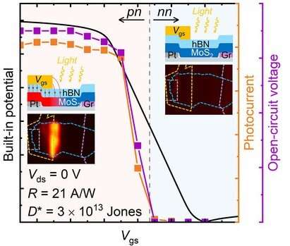
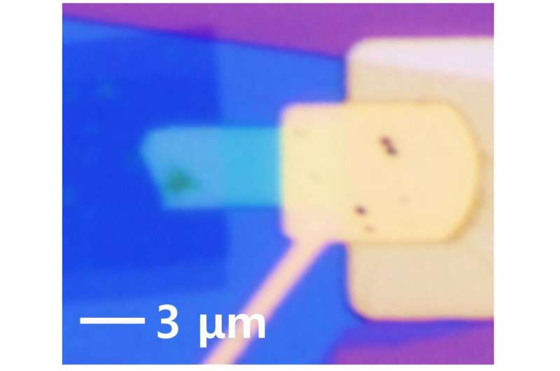
The team fabricated a PN junction structure photodetector capable of generating electrical signals on its own in environments with light, even without an electrical energy supply, by introducing a “van der Waals bottom electrode” that makes semiconductors extremely sensitive to electrical signals without doping.
A PN junction is a structure formed by joining p-type (hole-rich) and n-type (electron-rich) materials in a semiconductor. This structure causes current to flow in one direction when exposed to light, making it a key component in photodetectors and solar cells.
Normally, to create a proper PN junction, a process called doping is required, which involves deliberately introducing impurities into the semiconductor to alter its electrical properties. However, two-dimensional semiconductors such as MoS₂ are only a few atoms thick, so doping in the conventional way can damage the structure or reduce performance, making it difficult to create an ideal PN junction.

To overcome these limitations and maximize device performance, the research team designed a new device structure incorporating two key technologies: the van der Waals electrode and the partial gate.
The partial gate structure applies an electrical signal only to part of the two-dimensional semiconductor, controlling one side to behave like p-type and the other like n-type. This allows the device to function electrically like a PN junction without doping.
Furthermore, considering that conventional metal electrodes can chemically bond strongly to the semiconductor and damage its lattice structure, the van der Waals bottom electrode was attached gently using van der Waals forces. This preserved the original structure of the two-dimensional semiconductor while ensuring effective electrical signal transfer.
This approach secured both structural stability and electrical performance, enabling the realization of a PN junction in thin two-dimensional semiconductors without damaging their structure.

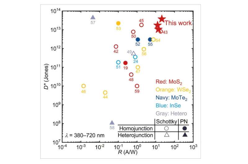
Thanks to this innovation, the team succeeded in implementing a high-performance PN junction without doping. The device can generate electrical signals with extreme sensitivity as long as there is light, even without an external power source. Its light detection sensitivity (responsivity) exceeds 21 A/W, more than 20 times higher than powered conventional sensors, 10 times higher than silicon-based self-powered sensors, and more than twice as high as existing MoS₂ sensors. This level of sensitivity means it can be applied immediately to high-precision sensors capable of detecting biosignals or operating in dark environments.
Professor Kayoung Lee said that they had “achieved a level of sensitivity unimaginable in silicon sensors, and although two-dimensional semiconductors are too thin for conventional doping processes, [they] succeeded in implementing a PN junction that controls electrical flow without doping.”
“This technology can be used not only in sensors, but also in key components that control electricity inside smartphones and electronic devices, providing a foundation for miniaturization and self-powered operation of next-generation electronics,” added Professor Lee.
More information:
Jaeha Hwang et al, Gated PN Junction in Ambipolar MoS2 for Superior Self‐Powered Photodetection, Advanced Functional Materials (2025). DOI: 10.1002/adfm.202510113
The Korea Advanced Institute of Science and Technology (KAIST)
Citation:
Self-powered photodetector achieves 20-fold sensitivity boost using novel device structure (2025, August 18)
retrieved 19 August 2025
from https://techxplore.com/news/2025-08-powered-photodetector-sensitivity-boost-device.html
This document is subject to copyright. Apart from any fair dealing for the purpose of private study or research, no
part may be reproduced without the written permission. The content is provided for information purposes only.

Comments are closed