Freestanding hafnium zirconium oxide membranes can enable advanced 2D transistors
To further reduce the size of electronic devices, while also improving their performance and energy efficiency, electronics engineers have been trying to identify alternative materials that outperform silicon and other conventional semiconductors. Two-dimensional (2D) semiconductors, materials that are just a few atoms thick and have a tunable electrical conductivity, are among the most promising candidates for the fabrication of smaller and better performing devices.
Past studies showed that these materials could be used to fabricate miniaturized transistors, electronic components that amplify or switch electrical signals, particularly field-effect transistors (FETs). These are transistors that control the flow of electrical current using an electric field.
To reliably operate, however, FETs also need to integrate an insulating layer that separates the so-called gate electrode (i.e., the terminal regulating the flow of current) from the channel (i.e., the pathway through which electrical current flows). To enable greater control over the gate, this insulating layer, known as a gate dielectric, should have a high dielectric constant (κ), or in other words, it should effectively store electrical energy.
Unfortunately, reliably integrating 2D semiconductors with high-κ insulators has so far proved difficult. This, along with other technical challenges, is currently preventing the widespread adoption of FETs based on 2D materials.
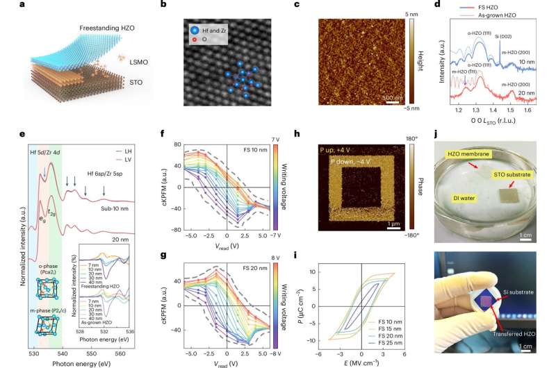
Researchers at National Chung Hsing, Kansai University, National Cheng Kung University and other institutes recently introduced a new strategy to reliably use freestanding membranes made of hafnium zirconium oxide (Hf0.5Zr0.5O2; HZO) as high- κ gate dielectrics in 2D FETs. Their proposed approach, outlined in a paper published in Nature Electronics, opens new possibilities for the creation of small and energy-efficient transistors, as well as highly performing logic-in-memory systems.
“2D semiconductors could be used as a channel material in miniaturized transistors with high gate control,” wrote Che-Yi Lin, Bo-Cia Chen and their colleagues in their paper. “However, the lack of insulators that are both compatible with two-dimensional materials and suitable for integration into a fully scalable process flow limits development. We show that freestanding Hf0.5Zr0.5O2 or HZO membranes can be integrated with two-dimensional semiconductors as a high-κ dielectric.”
As part of their study, the researchers first created freestanding HZO-based membranes. In this context, the term ‘freestanding’ means that the membranes do not need to be directly grown on a substrate, but can instead be transferred onto it independently.
“The HZO membranes can be varied in thickness from 5 to 40 nm, and be transferred onto molybdenum disulfide (MoS2) to create the top-gate dielectric in field-effect transistors,” wrote the authors.
“A 20-nm-thick HZO membrane exhibits a dielectric constant of 20.6 ± 0.5 and a leakage current (at 1 MV cm−1) of under 2.6 × 10⁻⁶ A cm−2, below the requirements of the International Technology Roadmap for Semiconductors, as well as typical ferroelectric behavior. The MoS2 transistors with HZO dielectric exhibit an on/off ratio of 109 and a subthreshold swing below 60 mV dec−1 across four orders of current.”
To demonstrate the potential of their fabrication strategy, the researchers used it to successfully create a variety of electronic components. The resulting devices were found to perform remarkably well, outperforming many 2D semiconductor-based electronic components developed in the past.
“We use the transistors to create an inverter, logic gates and a 1-bit full adder circuit,” wrote the authors. “We also create a MoS2 transistor with a channel length of 13 nm, which exhibits an on/off ratio of over 108 and a subthreshold swing of 70 mV dec−1.”
This recent study by Che-Yi Lin, Bo-Cia Chen and their colleagues, and the new approach they introduced, could contribute to the advancement of transistors and other devices based on 2D semiconductors. As part of their future studies, the researchers could refine their approach, while also further assessing its reliability and compatibility with existing electronics manufacturing processes.
Written for you by our author Ingrid Fadelli,
edited by Gaby Clark, and fact-checked and reviewed by Robert Egan—this article is the result of careful human work. We rely on readers like you to keep independent science journalism alive.
If this reporting matters to you,
please consider a donation (especially monthly).
You’ll get an ad-free account as a thank-you.
More information:
Che-Yi Lin et al, Integration of freestanding hafnium zirconium oxide membranes into two-dimensional transistors as a high-κ ferroelectric dielectric, Nature Electronics (2025). DOI: 10.1038/s41928-025-01398-y.
© 2025 Science X Network
Citation:
Freestanding hafnium zirconium oxide membranes can enable advanced 2D transistors (2025, July 31)
retrieved 1 August 2025
from https://techxplore.com/news/2025-07-freestanding-hafnium-zirconium-oxide-membranes.html
This document is subject to copyright. Apart from any fair dealing for the purpose of private study or research, no
part may be reproduced without the written permission. The content is provided for information purposes only.
Comments are closed