Strain engineering approach enhances performance of 2D semiconductor-based transistors
The manipulation of mechanical strain in materials, also known as strain engineering, has allowed engineers to advance electronics over the past decades, for instance enhancing the mobility of charge carriers in devices. Over the past few years, some studies have tried to devise effective strategies to manipulate strain in two-dimensional (2D) semiconductors that are compatible with existing industrial processes.
Researchers at Stanford University recently introduced a CMOS-compatible approach to engineer the tensile strain (i.e., stretchiness) in monolayer semiconductor transistors.
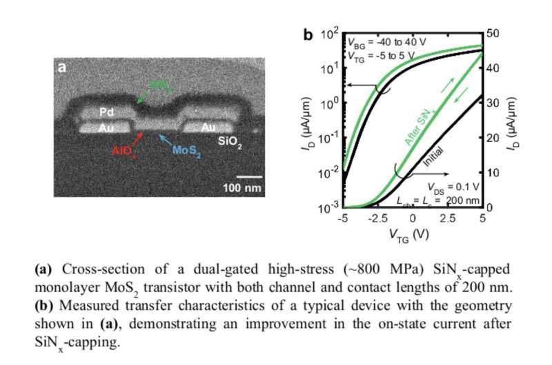
This approach, outlined in a paper published in Nature Electronics, relies on the use of silicon nitride capping layers that can impart strain on monolayer molybdenum disulfide (MoS2) transistors integrated on silicon substrates.
“We started brainstorming this idea as far back as 2020, when our research group was pursuing an earlier effort to apply strain by mechanically bending the samples,” Eric Pop, senior author of the paper, told Tech Xplore.
“At the time, there were very few experimental demonstrations of using strain to improve performance in two-dimensional (2D) material transistors, and none accomplished this using methods that are industry-friendly.
The main objective of the recent work by Pop and his colleagues was to try to identify new promising strain engineering techniques rooted in the processing of conventional silicon transistors, which could be applied to 2D materials. After delineating one of these techniques, they successfully applied it to a 2D MoS2-based transistor for the very first time.
“Drawing inspiration from the silicon industry in the early 2000s, our strategy uses thin silicon nitride capping layers (a material widely used in industry) to apply strain to the 2D semiconductor transistor,” explained Pop. “The stress in these films can be precisely tuned, and they can be deposited at relatively low temperatures, which is advantageous for various industrial applications.”
Firstly, the researchers processed 2D semiconductors using well-established fabrication techniques and used them to create transistors. They added silicon nitride films at the end of the processing, as this allowed them to clearly pin-point the effect these films had on the strain in the transistors, distinguishing it from effects linked to temperature changes and doping.
“The first notable contribution of this work is the experimental demonstration that process-induced strain (i.e. strain caused by various fabrication steps during transistor fabrication) exists in these 2D material transistors, and it can be leveraged to increase the on-state current using techniques which have been previously used for silicon transistors,” said Pop.
“Importantly, we also provided a simulation-based roadmap of how this strain changes as we shrink these devices to technologically-relevant dimensions, and found that strain holds great promise in this regime.”
In initial tests, the researchers found that their strain engineering approach enabled an enhancement in the performance of 2D MoS2 transistors, while also reducing both transistor channels and contacts. In the future, their work could contribute to the development of smaller and better performing 2D semiconductor-based transistors.
Meanwhile, Pop and his colleagues plan to continue testing and improving their proposed strain engineering technique. They also plan to investigate the effects of strain on other 2D semiconductors beyond monolayer MoS2.
“At the fundamental level, we are using flexible substrates to study the effect of strain in other 2D semiconductors which are less well-understood,” added Pop.
“Additionally, we are investigating other sources of process-induced strain such as the impact of metal deposition on 2D materials (a key step during device fabrication). Finally, we are working on extending this approach to p-type 2D transistors (as opposed to the n-type devices used in this study), because their performance currently lags behind that of the n-type devices.”
More information:
Marc Jaikissoon et al, CMOS-compatible strain engineering for monolayer semiconductor transistors, Nature Electronics (2024). DOI: 10.1038/s41928-024-01244-7.
© 2024 Science X Network
Citation:
Strain engineering approach enhances performance of 2D semiconductor-based transistors (2024, November 30)
retrieved 1 December 2024
from https://techxplore.com/news/2024-11-strain-approach-2d-semiconductor-based.html
This document is subject to copyright. Apart from any fair dealing for the purpose of private study or research, no
part may be reproduced without the written permission. The content is provided for information purposes only.

Comments are closed